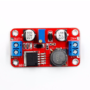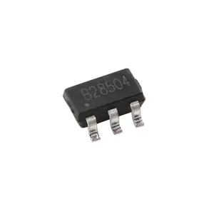
Explore our flagship OEM boost and buck-boost power converter platforms optimized for low-ripple, high power density, and broad input voltage stability.
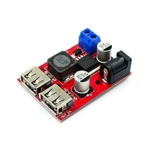
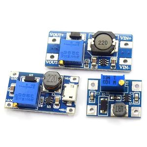
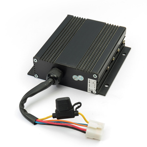
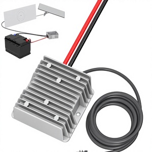
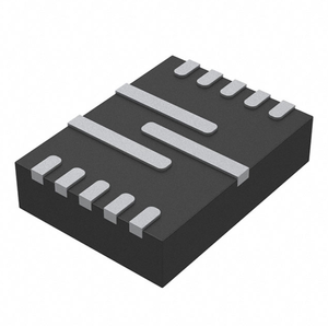
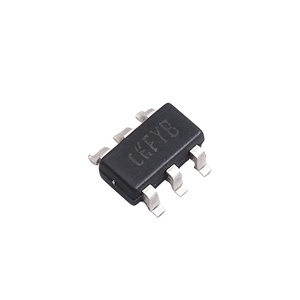
In modern electrical architectures—ranging from industrial automation switchgear and telecommunications remote units to electric vehicle (EV) sub-assemblies and satellite receiver systems—maintaining absolute DC voltage regulation across fluctuating input rails is a fundamental engineering prerequisite. As a specialized premier Custom OEM Boost Converter Manufacturer & Factory operated under Sanstar Microsystems Pvt. Ltd. (Micro Power), our engineering division has spearheaded the design, thermal optimization, EMI mitigation, and mass production of high-performance Switch Mode Power Supplies (SMPS) and step-up DC-DC converters since 1994.
Our industrial production facility operates full-scale surface mount technology (SMT) lines, custom magnetic component winding cells, anti-static (ESD-safe) assembly bays, and automated environmental stress screening (ESS) chambers. Unlike catalog distributors who merely rebrand standardized modules, our engineering methodology relies on first-principles power topology design. Whether your application demands a ultra-compact 2.5A surface-mount step-up converter IC, high-current synchronous rectification modules, or heavy-duty potted IP67 waterproof step-down/step-up regulators operating across severe ambient temperature gradients (-40°C to +85°C), Micro Power provides tailored OEM turn-key solutions built around your exact electrical and physical constraints.
A boost converter (step-up converter) is a DC-to-DC power converter that steps up voltage while stepping down current from its input supply to its output load. Achieving high efficiency, low electromagnetic interference (EMI), and minimal output voltage ripple requires rigorous design tradeoffs in power switch selection, magnetic circuit design, feedback loop compensation, and PCB layout parasitics.
Replacing traditional Schottky freewheeling diodes with ultra-low $R_{DS(on)}$ logic-level power MOSFETs drastically reduces conduction loss ($I^2 R$), driving conversion efficiencies beyond 96% even under heavy continuous current loads.
Custom-engineered ferrite-core inductors and planar transformers minimize magnetic flux leakage and skin-effect losses at elevated switching frequencies (up to 1.2MHz), constraining radiated EMI within CISPR 32 Class B limits.
Current-mode PWM architecture with high bandwidth error amplifiers ensures millisecond-level transient recovery time during step-load shifts, preventing supply rail sag in sensitive microcontroller and communication IC loads.
| Topology Parameter | Asynchronous Boost (XL6019 / MT3608) | Synchronous Step-Up (MP3431 / SY7072) | Integrated Buck-Boost (Auto-Regulated) |
|---|---|---|---|
| Typical Peak Efficiency | 90% - 93% | 95% - 98% | 91% - 94% |
| Input Voltage Window | 3.6V - 32V Wide Range | 0.8V Ultra-Low Start to 13V | 10V - 36V Wide Swing |
| Current Output Capacity | 2A - 5A Continuous | Up to 21A Peak Switching | 4.5A - 10A Constant Current/Voltage |
| Thermal Load Distribution | Diode absorbs heavy thermal dissipation | Balanced across high/low side MOSFETs | Requires aluminum plate/potting substrate |
| Target OEM Applications | General industrial, LED drivers, solar boost | Battery handhelds, high-density computing | Starlink Gen 3, automotive voltage stabilization |
The global DC-DC power converter market is undergoing a seismic migration toward higher power densities, electrification of transport, and decentralized green energy grids. Global procurement directors and enterprise hardware engineers must align their vendor qualification frameworks with three critical multi-year technology vectors:
Gallium Nitride (GaN) and Silicon Carbide (SiC) power devices are rapidly displacing traditional Silicon MOSFETs in high-power boost converters. GaN enables switching speeds exceeding 2MHz with near-zero reverse recovery charge ($Q_{rr}$). This allows OEM factories to reduce passive component sizes (inductors and ceramic capacitors) by up to 60%, delivering ultra-compact module footprints for space-constrained industrial housings.
With the global deployment of Low Earth Orbit (LEO) satellite networks (such as Starlink Gen 3 terminals), remote telecommunication enclosures require wide-input (10V-36V) step-up power supplies delivering clean, regulated 57V output at elevated current levels (4.5A+). OEM converters must integrate secondary surge suppression, reverse-polarity hardware protection, and thermal potting to survive extreme outdoor ambient exposures.
Procurement specifications for Industry 4.0 equipment increasingly mandate digitally managed power supplies. Modern boost converters now incorporate micro-telemetry ICs capable of transmitting real-time operating metrics—including input voltage, output current draw, internal junction temperature, and fault flags—directly to a master PLC via PMBus or I2C protocols for predictive maintenance.
To mitigate global supply disruptions, system integrators are moving away from single-source proprietary power modules. Enterprise buyers prioritize custom OEM factories capable of designing pin-to-pin drop-in compatible boost converter boards that adhere to standardized mechanical form factors while offering dual-sourced component footprints on the PCB level.
As the power electronics division of Sanstar Microsystems Pvt. Ltd. based in Nagpur, India, Micro Power brings over 30 years of uninterrupted design innovation, specialized engineering talent, and rigorous quality assurance frameworks to global OEM partners.
Our dedicated engineering board designs magnetics, multi-layer high-copper PCBs, thermal heat sinks, and firmware in-house. We transform initial customer load requirements into functional prototypes within rapid turn-around cycles.
Zero defect tolerance: 100% of manufactured boost modules undergo elevated-temperature burn-in testing under maximum load and automated high-voltage insulation tests prior to batch packaging.
Products manufactured in accordance with strict international safety standard frameworks including BIS (IS 13252), CE EMC directive compliance, and UL certification benchmarks for international market entry.
Analysis of input voltage window, peak/continuous output currents, ripple voltage limit, efficiency target, enclosure constraints, and target operating ambient.
SPICE electrical loop modeling, custom inductor core geometry calculations, planar magnetic design, and thermal finite element analysis (FEA).
Rapid SMT prototype execution followed by conducted/radiated EMI pre-compliance testing, surge immunity testing, and thermal imaging verification.
Automated SMT pick-and-place, selective soldering, conformal coating application, 100% ESS burn-in testing, and ERP-tracked global dispatch.
Modern boost converters utilize high-speed closed-loop Pulse Width Modulation (PWM) or Pulse Frequency Modulation (PFM) current-mode controllers. As the input voltage degrades (for example, a 12V lead-acid battery dropping to 10V under load), the internal feedback sense network automatically widens the switching duty cycle ($D = 1 - V_{in}/V_{out}$). This pulls higher input current through the primary energy storage inductor to maintain a rock-solid, regulated output voltage (e.g., 24V or 57V) until the under-voltage lockout (UVLO) threshold is reached.
Thermal management is executed across three engineering layers: First, power components (MOSFETs, diodes, inductors) are chosen with ultra-low internal resistances ($R_{DS(on)}$, $DCR$). Second, multi-layer 2oz or 3oz heavy-copper PCB layouts feature direct thermal via arrays under power pads to transfer heat to bottom-side aluminum heatsinks or enclosure walls. Third, for harsh environmental exposures, modules are encapsulated with thermally conductive silicone/epoxy potting compounds that eliminate hot spots and achieve IP67 ingress protection.
Non-isolated boost converters share a direct electrical ground path between the input supply and output load, maximizing energy conversion efficiency (often >95%) while minimizing physical size and cost. Galvanically isolated step-up converters utilize high-frequency transformers to break the ground loop, providing dielectric isolation (e.g., 1500V DC to 3000V AC). Isolated topologies are mandatory in railway, medical, high-voltage telecom, and utility switchgear applications where ground fault protection and noise immunity are legal mandates.
Niche platforms like Starlink Gen 3 dish terminals require precise 57V DC operating rails delivering up to 4.5A continuous power from standard 12V (10V–36V) mobile or solar battery sources. Micro Power designs custom step-up converter adapters incorporating specialized synchronous boost IC topologies, input reverse-polarity MOSFET switches, over-current latch protection, and customized low-resistance wiring harnesses to guarantee full system operational throughput without thermal throttling.
For standard catalog modules and minor board-level modifications, our MOQ starts as low as 100 units. For fully customized ground-up OEM power supply engineering (custom PCB layout, specialized housing, custom magnetics), prototype evaluation samples are typically delivered within 2 to 3 weeks following schematic sign-off, with full volume factory production lead times ranging from 4 to 6 weeks depending on component sourcing schedules.
Switching frequency is a primary trade-off parameter in power supply design. Higher switching frequencies (such as 1.2MHz used in ICs like the MT3608) allow for significantly smaller inductor values and smaller surface-mount ceramic output capacitors, creating ultra-compact module footprints. However, higher frequencies increase switching losses in power switch transistors. Lower frequencies (such as 150kHz used in XL6019 buck/boost platforms) offer superior switching efficiency and lower thermal stress, but require physically larger magnetic cores.
Consult directly with our senior power electronics engineering team to review your voltage stepping specifications, request custom prototype quotes, or schedule a factory audit.